The Brane SDK provides robust support for FPGA (Field-Programmable Gate Array) development, enabling hardware designers to create, simulate, and implement digital circuits using Hardware Description Languages (HDLs). This guide will walk you through creating a simple LED blinking circuit using Verilog and the Brane SDK’s FPGA toolchain integration.
Project Structure for FPGA Development #
An FPGA project in the Brane SDK follows this structure:
blinkingLeds/
├── build.gradle              # Configuration
└── src/
    ├── main/
    │   └── verilog/          # Main
    │       └── Blinking.v    # Top-level module
    └── test/
        └── verilog/          # Test bench
            ├── Test_Blinking.v  # Test bench
└── vector_test.txt # Test vectors 
Note: If you’ve completed previous tutorials in this guide, you’ll recognize the similar project organization approach. The main difference is using HDL-specific plugins and source directories.
Setting Up Your FPGA Project #
Let’s create a simple LED blinking circuit project:
Configure the Build File #
Add the following to your build.gradle file:
plugins {
    id 'com.brane.hdl'           // Core HDL plugin
    id 'com.brane.hdl.vivado'    // Xilinx Vivado integration
    //id 'com.brane.hdl.modelsim'  // Uncomment for ModelSim integration
}

HardwarePlugin {
    top = "Blinking"             // Top-level module name
    sim = "Test_Blinking"        // Test bench module name
    revision = "rev1"            // Hardware revision identifier
}

sourceSets {
    main {
        verilog {
            srcDirs += []        // Additional source directories if needed
        }
    }
    test {
        verilog {
            srcDirs += []        // Additional test directories if needed
        }
    }
}
This configuration:
- Applies the Brane SDK’s HDL plugins for Verilog development
- Specifies Xilinx Vivado as the implementation tool
- Defines the top-level module and test bench names
- Configures source directories for Verilog files
Implement the LED Blinking Circuit #
Add the following Verilog code to src/main/verilog/Blinking.v:
// Blinking LED Module

module Blinking (
    input clock_100,   // 100MHz clock input
    input reset_n,     // Active-low reset
    output led         // LED output signal
);

    // Internal registers
    reg [12:0] counter;  // 13-bit counter for timing
    reg state;           // LED state register

    // Connect state register to LED output
    assign led = state;

    // Sequential logic for counter and LED state
    always @ (posedge clock_100 or negedge reset_n)
    begin
        if (~reset_n) begin
            // Reset condition: initialize registers
            counter <= 0;
            state <= 0;
        end else begin
            // Normal operation: increment counter and update LED state
            counter <= counter + 1;
            state <= counter[12];  // Toggle LED based on counter MSB
        end
    end

endmodule
This simple circuit:
- Takes a 100MHz clock and reset signal as inputs
- Outputs a signal to drive an LED
- Uses a 13-bit counter to divide the clock frequency
- Toggles the LED state based on the most significant bit of the counter
Create the Test Bench #
Add the following test bench code to src/test/verilog/Test_Blinking.v:
`timescale 1 ns/10 ps  // time-unit = 1 ns, precision = 10 ps

module Test_Blinking;

    reg expected_led;
    wire led;
    reg reset_n;
    reg clock_100;

    // Test vector storage
    reg read_data [0:5];
    integer i;
    integer j;
    integer h;

    // Instantiate the design under test
    Blinking Blinkinh (
        .clock_100(clock_100),
        .reset_n(reset_n),
        .led(led)
    );

    // Generate Clock (50MHz)
    initial begin
        for (i = 0; i < 25000; i = i+1) begin
            clock_100 = 1'b0;
            #10000; // high for 20 * timescale = 20 ns

            clock_100 = 1'b1;
            #10000; // low for 20 * timescale = 20 ns
        end
        $finish;
    end

    // Generate reset_n
    initial begin
        reset_n = 1'b0;  // Assert reset
        #100000;         // Hold for 100 µs
        reset_n = 1'b1;  // Release reset
    end

    // Test sequence
    always @(posedge clock_100) begin
        if (reset_n) begin
            #20000;

            // Read test vectors from file
            $readmemb("../../src/test/verilog/vector_test.txt", read_data);

            // Check LED output against expected values
            for (j = 0; j < 6; j = j+1) begin
                expected_led = read_data[j];
                if (led == expected_led) begin
                    $display("led == expected_led");
                end else begin
                    $display("led %6d != expected_led %6d", led, expected_led);
                end

                // Wait for multiple clock cycles to see LED changes
                for (h = 0; h < 4096; h = h+1) begin
                    #20000;
                end
            end
        end
    end

endmodule : Test_Blinking
This test bench:
- Generates a 50MHz clock signal (20ns period)
- Applies a reset signal at the beginning of simulation
- Reads expected LED values from a test vector file
- Compares the actual LED output with expected values
- Reports any mismatches during simulation
Add Test Vectors #
Create a simple test vector file at src/test/verilog/vector_test.txt with alternating values:
0
1
0
1
0
1
These values represent the expected LED state at different times during simulation.
Building, Simulating, and executing the FPGA Design #
With the Brane SDK, building and simulating FPGA designs is streamlined through a comprehensive set of Gradle tasks that provide granular control over the development workflow:
Main Build (synthesis) Tasks #
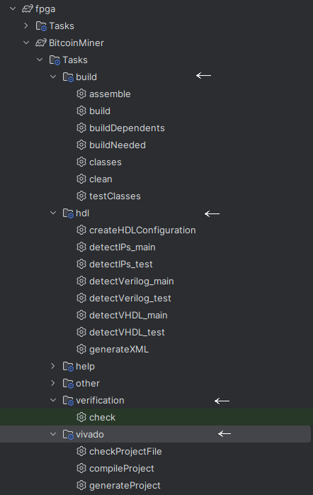
- Open the project in IntelliJ IDEA
- Navigate to the Gradle panel
- Expand Tasks > build
- Double-click on “build”
This command runs a full synthesis of the project and performs all tasks required to create a bitstream for the FPGA, including:
- Detecting all source files
- Generating project files for Vivado (or Quartus)
- Running compilation and synthesis
- Creating the final bitstream
Simulation #
- Open the project in IntelliJ IDEA
- Navigate to the Gradle panel
- Expand Tasks > verification
- Double-click on “check”
This command runs the simulation (using Vivado or ModelSim if active) to verify the functionality of your design against the test bench.
Expected output (build/synthesis) #
> Task :DevToolkit:tutorial:accelerators:fpga:blinkingLeds:compileProject

****** Vivado v2024.2 (64-bit)
  **** SW Build 5239630 on Fri Nov 08 22:34:34 MST 2024
  **** IP Build 5239520 on Sun Nov 10 16:12:51 MST 2024
  **** SharedData Build 5239561 on Fri Nov 08 14:39:27 MST 2024
  **** Start of session at: Mon Mar 24 14:08:20 2025
    ** Copyright 1986-2022 Xilinx, Inc. All Rights Reserved.
    ** Copyright 2022-2024 Advanced Micro Devices, Inc. All Rights Reserved.

source /tmp/compile_project5957342370603451830.tcl
# set step [lindex $argv 0]
# open_project /home/nicolas/Tools/brane-builder/brane-builder-plugin/DevToolkit/tutorial/accelerators/fpga/blinkingLeds/build/synthesis/Blinking.xpr

(...)

wait_on_runs: Time (s): cpu = 00:00:00.6 ; elapsed = 00:02:04 . Memory (MB): peak = 1386.414 ; gain = 0.000 ; free physical = 37405 ; free virtual = 84971
# if { $step == "bitstream" } {
#     # Generate bitstream
#     launch_runs impl_1 -to_step write_bitstream
#     wait_on_run impl_1
# }
# close_project
INFO: [Common 17-206] Exiting Vivado at Mon Mar 24 14:10:54 2025...

> Task :DevToolkit:tutorial:accelerators:fpga:blinkingLeds:build

Deprecated Gradle features were used in this build, making it incompatible with Gradle 9.0.

You can use '--warning-mode all' to show the individual deprecation warnings and determine if they come from your own scripts or plugins.

For more on this, please refer to https://docs.gradle.org/8.8/userguide/command_line_interface.html#sec:command_line_warnings in the Gradle documentation.

BUILD SUCCESSFUL in 2m 36s
12 actionable tasks: 8 executed, 4 up-to-date
2:10:54 PM: Execution finished 'build'.
By default, the synthesis of FPGA designs ends before the bitstream generation. You can overwrite the default behavior and also generate the bitstream in the options menu or Open Xilinx Vivado and generate the bitstream from Xilinx IDE.
Simulation #
You can simulate the design before or after the compilation depending on the simulator you use. If you use modelsim, you do not need to run a compilation. If you use Vivado, you will have to run a compilation. Then simply run the simulation using “check”.

Understanding the FPGA Development Flow #
The FPGA development process in the Brane SDK follows a standard flow with several key stages:
RTL Design #
Register Transfer Level (RTL) design involves writing hardware description code that specifies:
- The behavior of your circuit
- The registers and signals that store and transfer data
- The combinational logic that processes data
In our example, the Blinking.v file describes a counter-based LED controller at the RTL level.
Functional Simulation #
Before synthesis, you verify the logical behavior of your design through simulation:
- A test bench provides stimulus to your design
- The simulator executes your code and tracks signal changes
- Test vectors and assertions verify correct behavior
Our Test_Blinking.v test bench simulates the LED blinking circuit and checks its output against expected values.
Synthesis #
During synthesis, the RTL description is converted to a gate-level netlist:
- The tool maps your HDL code to available FPGA resources (LUTs, flip-flops, etc.)
- Optimizations are applied to meet timing and area constraints
- A gate-level netlist is generated representing your circuit
The Brane SDK handles synthesis automatically when you run the build task.
Implementation #
The implementation phase maps your design to the specific FPGA device:
- Place: Assigns netlist elements to physical locations on the FPGA
- Route: Creates connections between placed elements
- Timing analysis: Verifies that signals meet timing requirements
The build task manages this process, producing detailed reports about resource usage and timing.
Bitstream Generation #
The final step generates a bitstream file that configures the FPGA:
- The bitstream contains the configuration data for all FPGA elements
- This file is used to program the FPGA device
- After programming, the FPGA immediately begins executing your design
Code and Implementation Explained #
Let’s examine the key components of our LED blinking example in more detail:
Verilog Module Analysis #
The Blinking module implements a simple digital circuit:
module Blinking (
    input clock_100,   // 100MHz clock input
    input reset_n,     // Active-low reset
    output led         // LED output signal
);
This module declaration defines:
- Two input ports: a clock signal and an active-low reset
- One output port: the LED control signal
The internal counter and state registers are declared as:
reg [12:0] counter;  // 13-bit counter for timing
reg state;           // LED state register
The counter register is 13 bits wide, allowing it to count from 0 to 8,191 before overflowing back to 0. This creates a time delay between LED state changes.
The continuous assignment connects the internal state register to the output:
assign led = state;The sequential logic block handles the counter and LED state updates:
always @ (posedge clock_100 or negedge reset_n)
begin
    if (~reset_n) begin
        // Reset condition
        counter <= 0;
        state <= 0;
    end else begin
        // Normal operation
        counter <= counter + 1;
        state <= counter[12];
    end
end
This block:
- Executes on every rising edge of the clock or falling edge of reset
- Resets both registers to 0 when reset_n is low
- Increments the counter on each clock cycle
- Sets the LED state based on the most significant bit (MSB) of the counter
Since the MSB of the counter (bit 12) toggles after 2^12 = 4,096 clock cycles, the LED will toggle at a much lower frequency than the input clock, creating a visible blinking effect.
Test Bench Analysis #
The test bench creates a virtual environment to test the LED blinking circuit:
// Instantiate the design under test
Blinking Blinkinh (
    .clock_100(clock_100),
    .reset_n(reset_n),
    .led(led)
);
This instantiates the Blinking module and connects it to signals in the test bench.
The clock generation block creates a 50MHz clock signal:
// Generate Clock (50MHz)
initial begin
    for (i = 0; i < 25000; i = i+1) begin
        clock_100 = 1'b0;
        #10000; // 10ns low
        clock_100 = 1'b1;
        #10000; // 10ns high
    end
    $finish;
end
The reset generation applies an initial reset pulse:
// Generate reset_n
initial begin
    reset_n = 1'b0;  // Assert reset
    #100000;         // Hold for 100 µs
    reset_n = 1'b1;  // Release reset
end
The test sequence checks the LED output against expected values:
always @(posedge clock_100) begin
    if (reset_n) begin
        #20000;

        // Read test vectors from file
        $readmemb("../../src/test/verilog/vector_test.txt", read_data);

        // Verification loop
        for (j = 0; j < 6; j = j+1) begin
            expected_led = read_data[j];
            // Check actual vs expected
            ...
            // Wait for LED changes
            ...
        end
    end
end
This block:
- Waits for reset to be released
- Reads expected LED values from a file
- Compares the actual LED output with expected values
- Waits between comparisons to allow the LED state to change
Build Configuration Analysis #
The build.gradle file configures the FPGA development tools:
plugins {
    id 'com.brane.hdl'           // Core HDL plugin
    id 'com.brane.hdl.vivado'    // Xilinx Vivado integration
}
These plugins provide:
- Support for HDL compilation and simulation
- Integration with Xilinx Vivado for synthesis and implementation
- Automated project setup and tool configuration
The HardwarePlugin block specifies key parameters for the FPGA project:
HardwarePlugin {
    top = "Blinking"             // Top-level module name
    sim = "Test_Blinking"        // Test bench module name
    revision = "rev1"            // Hardware revision identifier
}
This configuration:
- Identifies the top-level module for synthesis (
Blinking) - Specifies the test bench module for simulation (
Test_Blinking) - Assigns a revision identifier for version tracking
The sourceSets block configures source file directories:
sourceSets {
    main {
        verilog {
            srcDirs += []        // Additional source directories if needed
        }
    }
    test {
        verilog {
            srcDirs += []        // Additional test directories if needed
        }
    }
}
This allows you to specify additional source directories beyond the default locations if needed for larger projects.
Optimizing FPGA Designs #
To improve your FPGA designs, consider these optimization strategies:
Efficient Use of FPGA Resources #
FPGAs have limited resources of different types:
- Look-Up Tables (LUTs) for implementing logic functions
- Flip-Flops (FFs) for storing state
- Block RAMs for larger memory arrays
- DSP blocks for arithmetic operations
Optimize your design to balance resource usage and meet your performance goals.
Clock Domain Management #
Proper clock domain design is crucial for reliable FPGA operation:
- Minimize the number of clock domains to reduce complexity
- Use appropriate clock crossing techniques between domains
- Understand timing constraints and setup/hold times
The Brane SDK helps manage clock domains through automated constraint generation.
Pipelining for Performance #
Pipelining divides operations into stages separated by registers:
- Increases throughput by allowing multiple operations in flight
- Improves timing by breaking long paths into shorter segments
- Enables higher clock frequencies
For complex designs, pipelining is often essential to meet timing requirements.
Timing Closure #
Meeting timing requirements is crucial for reliable FPGA operation:
- Review timing reports to identify critical paths
- Add pipeline registers to break long combinational paths
- Consider using clock enables instead of gated clocks
- Specify appropriate timing constraints
The Brane SDK generates detailed timing reports to help with this process.
Common Issues and Solutions #
| Issue | Possible Cause | Solution |
| Simulation mismatch | Incorrect test vectors or design logic | Review test bench and design logic, check signal timing |
| Synthesis failure | Unsupported HDL constructs | Modify code to use synthesizable constructs |
| Timing violations | Long combinational paths | Add pipeline registers, optimize logic |
| Resource constraints | Design too large for target FPGA | Optimize resource usage, consider a larger FPGA |
| Implementation errors | Tool configuration issues | Check constraint files and tool settings |
Next Steps #
To further develop your FPGA skills with the Brane SDK:
- Explore more complex designs such as state machines, memory interfaces, or arithmetic units
- Create larger hierarchical designs using multiple modules
- Implement communication interfaces like UART, SPI, or AXI
- Integrate with software using processor cores and memory-mapped interfaces
- Learn about advanced verification techniques using SystemVerilog assertions


